
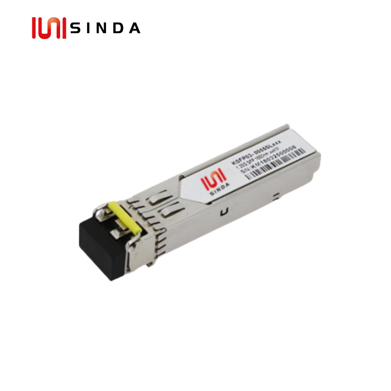
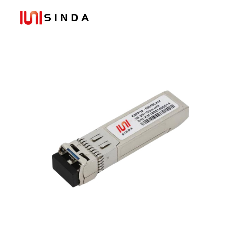
1.25Gb/s SFP 1550nm Duplex 80Km Transceiver,SSFP03-0055SL80X Small Form Factor Pluggable (SFP) transceivers are compatible with theSmall Form Factor Pluggable Multi-Sourcing Agreement (MSA). The transceiver consists of five sections: the LD driver, the limiting amplifier, the digital diagnostic monitor, the 1550nm DFB laser and the PIN photo-detector .The module data link up to 80KM in 9/125um single mode fiber.


1.25Gb/s SFP 1550nm Duplex 80Km Transceiver
The optical output can be disabled by a TTL logic high-level input of Tx Disable, and the system also can disable the module via I2C. Tx Fault is provided to indicate that degradation of the laser. Loss of signal (LOS) output is provided to indicate the loss of an input optical signal of receiver or the link status with partner. The system can also get the LOS (or Link)/Disable/Fault information via I2C register access.
Products Features
Up to 1.25Gb/s data links
DFB laser transmitter and PIN photo-detector
Up to 80km on 9/125µm SMF
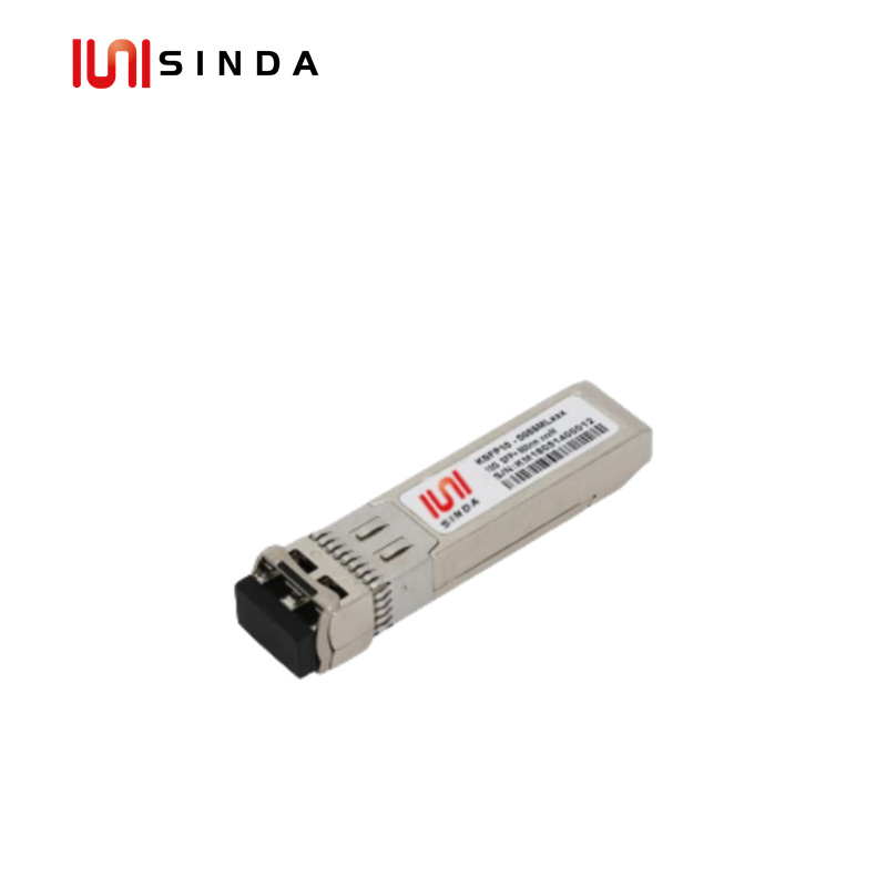
Hot-pluggable SFP footprint
Duplex LC/UPC type pluggable optical interface
Low power dissipation
Metal enclosure, for lower EMI
RoHS compliant and lead-free
Single +3.3V power supply
Support Digital Diagnostic Monitoring interface
Compliant with SFF-8472
Case operating temperature
Commercial: 0°C to +70°C
Industrial: -40°C to +85°C
Applications
Switch to Switch Interface
Gigabit Ethernet
Switched Backplane Applications
Router/Server Interface
Other Optical Links
Pin Description.
| Pin | Symbol | Name/Description | NOTE |
| 1 | VEET | Transmitter Ground (Common with Receiver Ground) | 1 |
| 2 | TFAULT | Transmitter Fault. | |
| 3 | TDIS | Transmitter Disable. Laser output disabled on high or open. | 2 |
| 4 | MOD_DEF(2) | Module Definition 2. Data line for Serial ID. | 3 |
| 5 | MOD_DEF(1) | Module Definition 1. Clock line for Serial ID. | 3 |
| 6 | MOD_DEF(0) | Module Definition 0. Grounded within the module. | 3 |
| 7 | Rate Select | No connection required | 4 |
| 8 | LOS | Loss of Signal indication. Logic 0 indicates normal operation. | 5 |
| 9 | VEER | Receiver Ground (Common with Transmitter Ground) | 1 |
| 10 | VEER | Receiver Ground (Common with Transmitter Ground) | 1 |
| 11 | VEER | Receiver Ground (Common with Transmitter Ground) | 1 |
| 12 | RD- | Receiver Inverted DATA out. AC Coupled | |
| 13 | RD+ | Receiver Non-inverted DATA out. AC Coupled | |
| 14 | VEER | Receiver Ground (Common with Transmitter Ground) | 1 |
| 15 | VCCR | Receiver Power Supply | |
| 16 | VCCT | Transmitter Power Supply | |
| 17 | VEET | Transmitter Ground (Common with Receiver Ground) | 1 |
| 18 | TD+ | Transmitter Non-Inverted DATA in. AC Coupled. | |
| 19 | TD- | Transmitter Inverted DATA in. AC Coupled. | |
| 20 | VEET | Transmitter Ground (Common with Receiver Ground) | 1 |
Notes:
1. Circuit ground is internally isolated from chassis ground.
2. Laser output disabled on TDIS >2.0V or open, enabled on TDIS <0.8V.
3. Should be pulled up with 4.7k - 10kohms on host board to a voltage between 2.0V and 3.6V.MOD_DEF (0) pulls line low to indicate module is plugged in.
4. This is an optional input used to control the receiver bandwidth for compatibility with multiple data rates (most likely Fiber Channel 1x and 2x Rates).If implemented, the input will be internally pulled down with > 30kΩ resistor. The input states are:
Ÿ Low (0 – 0.8V): Reduced Bandwidth
Ÿ (>0.8, < 2.0V): Undefined
Ÿ High (2.0 – 3.465V): Full Bandwidth
Ÿ Open: Reduced Bandwidth
5. LOS is open collector output should be pulled up with 4.7k - 10kohms on host board to a voltage between 2.0V and 3.6V. Logic 0 indicates normal operation; logic 1 indicates loss of signal.


-----------------------------
Quality Certification

 NO.4007,Peanut U Gu Creative Park , No.57 GuangDa Rd,LongGang Zone, Shenzhen city, China.
 Copyright @ 2026 Shenzhen Sinda Optic Technology Co.,ltd All Rights Reserved.
 Network Supported
Sitemap | Blog | Xml | Privacy Policy
 English
 español
 العربية
 Kiri Shigawara