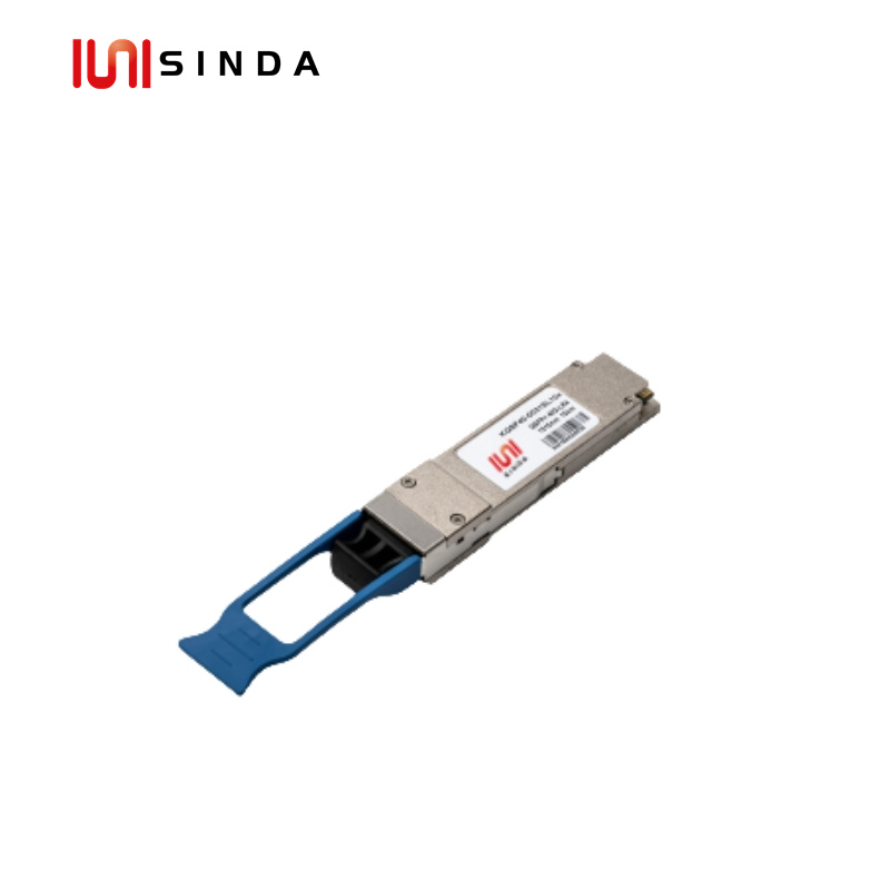
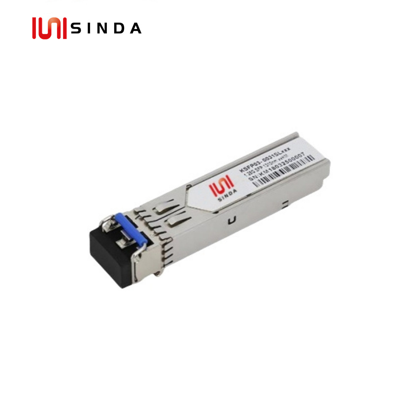
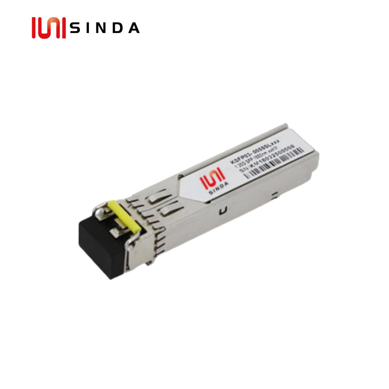
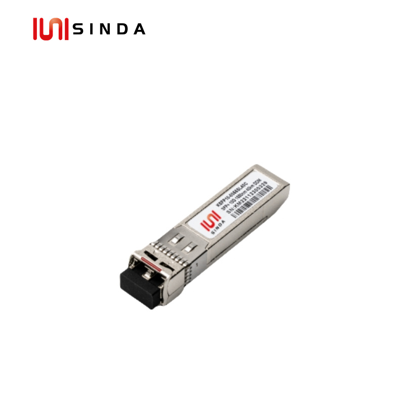
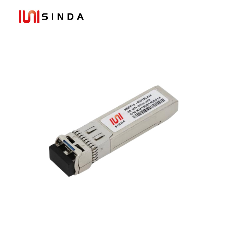
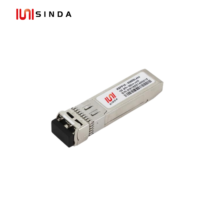
40Gbps QSFP+ LR4 10km Optical Transceiver,This product is a 40G QSFP+ LR4 integrates four transmitters and receivers into one module. The central wavelengths of the channels are 1271, 1291, 1311 and 1331 nm as members of the CWDM wavelength grid defined in ITU-T G.694.2.


40Gbps QSFP+ LR4 10km Optical Transceiver
In the transmitter side, the four lanes of optical data channels are optically multiplexed by the integrated optical multiplexer. In the receive side, the four lanes of optical data channels are optically de-multiplexed by the integrated optical de-multiplexer. Each data channels is recovered by a PIN photo-detector and trans-impedance amplifier, retimed.
The product is designed with form factor, optical/electrical connection and digital diagnostic interface according to the QSFP+ IEEE802.3ba 40GBASE-LR4 and compliant to SFF-8436.
Products Features
Hot pluggable QSFP+ MSA form factor
Supports 41.25Gb/s aggregate bit rate
Integrated 4 CWDM lanes MUX/DEMUX
Up to 10km transmission on single mode fiber (SMF)
XLPPI electrical interface
Duplex LC receptacles
Hot pluggable QSFP+ form factor
Maximum power consumption 3.5W
Case operating temperature range:0℃~+70℃
RoHS Compliant
DDMI function available with internally calibrated mode
I2C management interface
Applications
Data Center
Ethernet Switches
Pin Description.
| Pin | Symbol | Name/Description | NOTE |
| 1 | GND | Transmitter Ground (Common with Receiver Ground) | 1 |
| 2 | Tx2n | Transmitter Inverted Data Input | |
| 3 | Tx2p | Transmitter Non-Inverted Data output | |
| 4 | GND | Transmitter Ground (Common with Receiver Ground) | 1 |
| 5 | Tx4n | Transmitter Inverted Data Input | |
| 6 | Tx4p | Transmitter Non-Inverted Data output | |
| 7 | GND | Transmitter Ground (Common with Receiver Ground) | 1 |
| 8 | ModSelL | Module Select | |
| 9 | ResetL | Module Reset | |
| 10 | VccRx | 3.3V Power Supply Receiver | 2 |
| 11 | SCL | 2-Wire serial Interface Clock | |
| 12 | SDA | 2-Wire serial Interface Data | |
| 13 | GND | Transmitter Ground (Common with Receiver Ground) | |
| 14 | Rx3p | Receiver Non-Inverted Data Output | |
| 15 | Rx3n | Receiver Inverted Data Output | |
| 16 | GND | Transmitter Ground (Common with Receiver Ground) | 1 |
| 17 | Rx1p | Receiver Non-Inverted Data Output | |
| 18 | Rx1n | Receiver Inverted Data Output | |
| 19 | GND | Transmitter Ground (Common with Receiver Ground) | 1 |
| 20 | GND | Transmitter Ground (Common with Receiver Ground) | 1 |
| 21 | Rx2n | Receiver Inverted Data Output | |
| 22 | Rx2p | Receiver Non-Inverted Data Output | |
| 23 | GND | Transmitter Ground (Common with Receiver Ground) | 1 |
| 24 | Rx4n | Receiver Inverted Data Output | 1 |
| 25 | Rx4p | Receiver Non-Inverted Data Output | |
| 26 | GND | Transmitter Ground (Common with Receiver Ground) | 1 |
| 27 | ModPrsl | Module Present | |
| 28 | GND | Transmitter Ground (Common with Receiver Ground) | |
| 29 | Tx2n | Transmitter Inverted Data Input | 2 |
| 30 | Tx2p | Transmitter Non-Inverted Data output | 2 |
| 31 | GND | Transmitter Ground (Common with Receiver Ground) | |
| 32 | Tx4n | Transmitter Inverted Data Input | 1 |
| 33 | Tx4p | Transmitter Non-Inverted Data output | |
| 34 | GND | Transmitter Ground (Common with Receiver Ground) | |
| 35 | ModSelL | Module Select | 1 |
| 36 | ResetL | Module Reset | |
| 37 | VccRx | 3.3V Power Supply Receiver | |
| 38 | SCL | 2-Wire serial Interface Clock | 1 |
Notes:
1. GND is the symbol for signal and supply (power) common for QSFP+ modules. All are common within the QSFP+ module and all module voltages are referenced to this potential unless otherwise noted. Connect these directly to the host board signal common ground plane.
2. VccRx, Vcc1 and VccTx are the receiver and transmitter power suppliers and shall be applied concurrently. Recommended host board power supply filtering is shown in Figure 4 below. Vcc Rx, Vcc1 and Vcc Tx may be internally connected within the QSFP+ transceiver module in any combination. The connector pins are each rated for a maximum current of 1000mA.
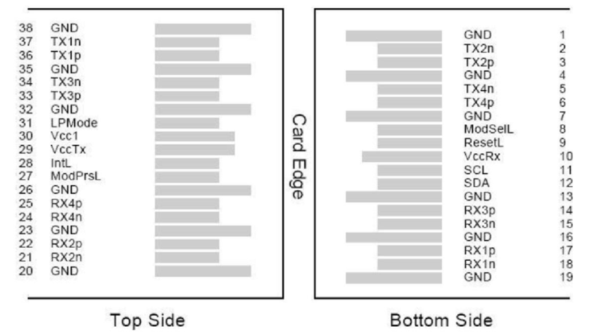
Pin-out of Connector Block on Host Board
Quality Certification

 NO.4007,Peanut U Gu Creative Park , No.57 GuangDa Rd,LongGang Zone, Shenzhen city, China.
 Copyright @ 2026 Shenzhen Sinda Optic Technology Co.,ltd All Rights Reserved.
 Network Supported
Sitemap | Blog | Xml | Privacy Policy
 English
 español
 العربية
 Kiri Shigawara